

全新3D PCSEL模型的初测版本已发布,并集成到PICS3D 2024 试用版中。
感兴趣的用户可以联系Crosslight获取相关试用版本。
获取资料进一步了解该PCSEL模拟功能的介绍:Crosslight_3D_PCSEL_zh.pdf
山东大学刘超课题组使用Crosslight公司的APSYS软件在器件仿真课题多个项目上取得了令人瞩目的研究成果。
以下分享课题组在2023年及2024年发表的多项学术论文:
Paper1:
Paper2:
《Analytical Model and Design Strategy for GaN Vertical Floating Island Schottky Diodes》
Paper3:
Paper4:
Paper5:
Paper6:
Paper7:
Paper8:
《Enhanced hole injection in Ga-polar 290 nm AlGaN-based DUV LEDs with a p-n junction hole accelerator》
Paper9:
Paper10:
Paper11:
Paper12:
Paper13:
Paper14:
Crosslight即将发布2023最新正式版软件,其中包含诸多具有里程碑意义的崭新功能;新版本除了在现有版本的基础上进一步改进和优化之外,还包含了以下新特性:
氧化限制性VCSEL模型的新示例已经上传。演示了微腔模型计算的多模分布以及最近添加到 PICS3D 测试版中新的光谱分析功能。感兴趣的试用用户,和仍在技术支持合约有效期内的客户可以联系我们,以便尽早获取2023测试版和运行此示例所需的文件。
从2023版本开始,SiGe调制器的新模型已添加到我们的标准PICS3D示例库中。感兴趣的试用用户,和仍在技术支持合约有效期内的客户可以联系我们,以便尽早获取2023测试版和运行此示例所需的文件。
高对比度光栅晶体垂直面发射激光器(HCG-VCSEL)的新模型,已经为我们的PICS3D测试版示例,使用了麦克斯韦方程的矢量FDFD求解器中最新改进的功能。感兴趣的试用用户,和仍在技术支持合约有效期内的客户可以联系我们,以便尽早获取2023测试版和运行此示例所需的文件。
利用我们在麦克斯韦方程矢量FDFD求解器中的最新改进,我们的PICS3D测试版演示了光子晶体垂直面发射激光器(PC-VCSEL)模型的新模型。感兴趣的试用用户,和仍在技术支持合约有效期内的客户可以联系我们,以便尽早获取2023测试版和运行此示例所需的文件。
我们很荣幸地宣布与伊利诺伊大学厄巴纳-香槟分校助理教授Can Bayram合作的第四位年度获奖者。作为此次合作的一部分,学生们在学术环境中使用Crosslight TCAD工具,并获得了最佳项目。
祝贺2023年度获奖者:
NITHIYASSRI K R T VIVAGANDAN Designing Blue-Wavelength Free White Light: A Dichromatic Approach Using Violet and Yellow-Green LEDs
我们很荣幸地宣布与伊利诺伊大学厄巴纳-香槟分校助理教授Can Bayram合作的第四位年度获奖者。作为此次合作的一部分,学生们在学术环境中使用Crosslight TCAD工具,并获得了最佳项目。
祝贺2022年该奖项的获奖者:
Jaekwon Lee for 2D Optical-Thermal-Electrical Simulation for High Wall Plug Efficiency Cubic GaN Green LED on Silicon
Robert Kaufman for HgCdTe Long-Wave Infrared Photovoltaics for Directed Energy Applications
我们的首席执行官兼创始人Simon Li博士在CASICON2021会议上发表的演讲副本,已上传到我们的杂项会议页面。
Crosslight很荣幸地宣布,即将发布的2021版本的新功能里程碑。除了修复多个错误和改进外,进行了新功能和改进:
这个版本将在今年晚些时候最终测试完成后发布。仍在技术支持合约有效期内的客户如果希望立即尝试这些新功能,可以联系当地的销售代表。
我们很荣幸地宣布与伊利诺伊大学厄巴纳-香槟分校助理教授Can Bayram合作的第四位年度获奖者。作为此次合作的一部分,学生们在学术环境中使用Crosslight TCAD工具,并获得了最佳项目。
祝贺2021年该奖项的获奖者:
Yu-Chieh Chiu for “Designing Efficient Micro Light Emitting Diodes for Display Applications”
Jonah Messinger for “Harnessing Cobalt-60 Gamma Radiation with ZnTe Gammavoltaic Devices and an LuI3 Scintillator Interface for Clean Firm Power Generation”.
Three-dimensional (3D) modeling is reported for CMOS active pixel image sensors particularly by comparing frontsurface and back-surface illumination. The opto-electronic responses are presented versus various power intensity and illumination wavelength.
The optical efficiency and quantum efficiency from FDTD modeling are also presented. For appropriately designed sensor structure, it is shown that back-surface illumination pixel could achieve improved sensitivity within certain wavelength range.
The presented results demonstrate a methodological and technical capability for 3D modeling optimization of complex CMOS image sensor.
Keywords:
CMOS image sensor, active pixel sensor, optoelectronics, device modeling and TCAD software, semiconductor devices
The complementary metal oxide semiconductor (CMOS) image sensors (CIS) are being widely used in various camera systems for automotive, consumer, industrial, & security imaging applications. The active pixel sensor (APS) has attracted increasing interest due to demand for miniaturized system-on-chip capability, low-power, and cost-effective imaging systems during the past two decades [1-3].
To increase the sensitivity without compromising the resolution for a front-surface illuminated (FSI) image sensor, various approaches including several photodiode structures such as the pinned photodiode (PPD) [3,4] have been proposed. Micro lens has also been fabricated to increase the light gathering power [5].
Other means like increasing the fill factor of the photo-electric conversion element as well as increasing the conversion gain of the source-follower amplifier etc have also been explored.
As a further technical development to overcome the benefit limitation of the aforementioned approaches, the back-surface illuminated (BSI) image sensor has attracted increasing attention due to enhanced sensitivity [6,7] and improved low-light performance.
It has been noted that a BSI sensor could theoretically cost less than a similar FSI one with the ability to collect more light.
For a similarly sized sensor to FSI one, the BSI array could offer higher resolution without the drop in low-light performance. Alternatively, for the same resolution and low-light capability, the BSI sensor could be achieved on a smaller chip with reduced costs. The BSI sensors have entered the commercialization market in recent years.
Due to the complexity of the 3D integration of photodiode and the optimization of metal layer distribution to maximize the sensitive area, 3D modeling together with effective optical modeling method such as finite difference time domain (FDTD) technique is indispensable [8,9]. An effective 3D modeling tool kit with full breadth covering process, optical and opto-electric response modeling is definitely requested.
In this work, based on Crosslight CSuprem and APSYS [10], we present 3D modeling of APS units designed for comparing the opto-electronic response between FSI and BSI pixels.
The paper is organized as flows. In section 2, brief software and methodological background for the modeling is described. In section 3, comparison is presented between two individual sensor pixels, one for FSI and the other for BSI, which are built by Crosslight LayerBuilder and simulated by APSYS.
Further in section 4, comparing results are presented between FSI and BSI for one individual sensor pixel, which is built and process simulated by Crosslight Csuprem together with Crosslight APSYS for the modeling the opto-electronic response. Summary and conclusion is finally given in section 5.
2.1 Software background
The Crosslight CSuprem [10] is a powerful 2D/3D process simulator, which is capable to interface with Crosslight APSYS. Its features include ion implantation, anisotropic and sacrificial etching, deposition, diffusion, annealing and oxidation etc. The Crosslight APSYS is general-purpose 2D/3D finite element analysis and modeling software for semiconductor devices [10].
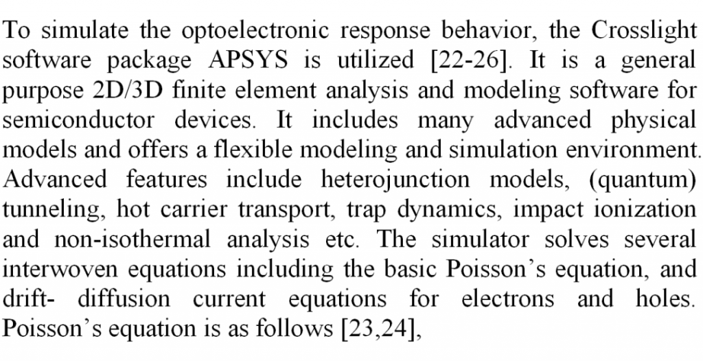
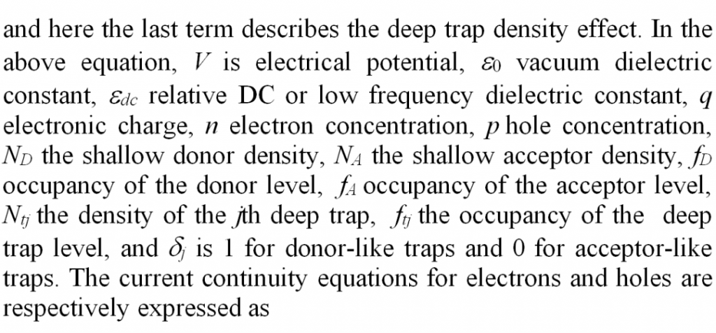
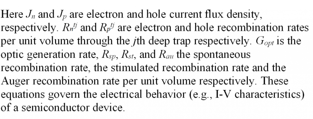
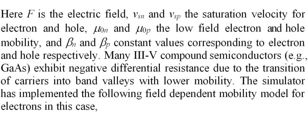
The simulator solves several interwoven equations including the basic Poisson’s equation, and drift-diffusion current equations for electrons and holes. It includes many advanced physical models, friendly-using features and offers a flexible modeling and simulation environment. Advanced models include heterojunction models, (quantum) tunneling, hot carrier transport, trap dynamics, impact ionization and non-isothermal analysis etc. Important generation and recombination mechanisms, such as Shockley-Reed-Hall, spontaneous and Auger recombination, are taken into account. The software simulator provides several mobility model options from constant values to field dependent ones.
To simulate the optical effect of the complex CIS structure, Crosslight FDTD as well as interface techniques to other FDTD software is developed with APSYS. The graphic processing unit (GPU) solver is also implemented for fast computation capability.
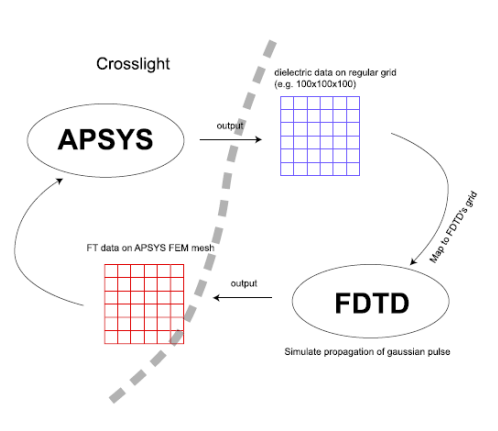
The schematic interface between FDTD and Crosslight APSYS is shown in Fig. 1 (a) [9].
The 3D grid uniform in each coordinate direction must be used for FDTD so there is a mapping of irregular device structure finite element data from/to Crosslight APSYS. In this work, all the optical efficiency (OE) and quantum efficiency (QE) results are from FDTD simulation of the relevant CIS structures. The OE is defined as the integration of the ratio of (ingoing flux-outgoing flux)/incident flux over device interface, where ingoing flux is the difference between the incident flux and the reflected flux upon the very beginning surface illuminated first. The QE is defined as integration of (absorption rate)*(relative energy intensity) across all the device 3D grid points. The OE does not care about which material absorbs light and has electron-hole pairs generated. The QE computation involves in more mesh memory than OE but provides more insight on the photo-electric conversion efficiency than the OE. The opto-electric response modeling like various contact terminal potential evolution versus operating time cycle is solely based on Crosslight APSYS with optical model involving in transfer matrix method (TMM) unless specified with alternative means.
2.2 Forming 3D CIS structures
The 3D CIS structures could be either formed by Crosslight LayerBuilder with multi-layers/columns by taking the advantage of the 3D-connect flow option. The 3D CIS formed by this way does not involve in process simulation. The 3D CIS structures could also be partially or fully process-built and simulated by Crosslight CSuprem with structure mesh, material together with doping exported and interfaced to Crosslight APSYS.
The latter is often used for complicated irregular geometrical design involving in multiple mask sets as designed by Crosslight Maskeditor. The schematic APS unit structure is similar to Ref. [1-3,5,7,9] including a pinned photodiode, a transfer (TX) gate, and a reset (RST) gate.
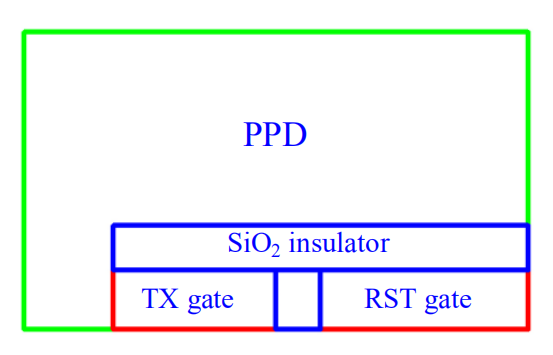
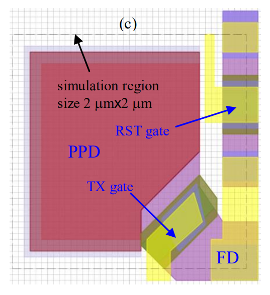
Due to the thinning request and also for reducing the mesh size, we assume 5-um-thick p-type starting substrate. The typical CIS schematic (regular geometry) with Crosslight LayerBuilder only is shown in Fig. 1 (b) whereas the detailed unit component deployment (as generated by Crosslight MaskEditor with 9 mask layers and subsequent CSuprem process simulation) is schematically shown in Fig. 1 (c).
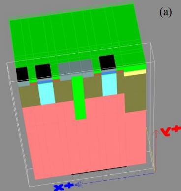
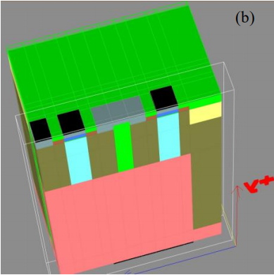
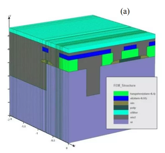
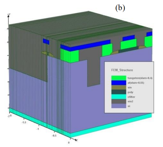
In this section, we compare two sensor structures, one for FSI and the other for BSI. These two pixels are built by APSYS LayerBuilder only according to the schematics shown in Fig. 1 (b). These two structures with 3D connect-flow are shown in Fig. 2 (a) and (b) for FSI and BSI, respectively. Trench insulators are inserted among PPD, TX gate and RST gate. Most of the front surface is simply assumed to be covered with thin SiO2 as anti-reflection coating layer whereas the back surface is the (thinned) wafer base. For simplicity, no color filter array (CFA) is included for these two structures for most of the modeling work except for comparison presented at the end of this section.
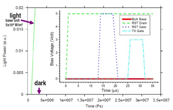
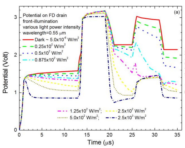
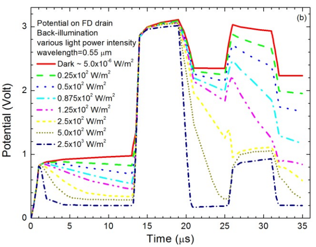
With the operating illumination and bias time clock cycle (reset at first and then transfer) as shown in Fig. 3, the evolution of the potential on the floating drain (FD) versus time is shown in Fig. 4 (a) and (b) respectively for FSI and BSI pixel, respectively. With increasing power intensity, the potential on FD shows increasingly large difference relative to the dark case at the transfer stage. When the power intensity reaches certain level, the overshot-effect becomes dominant at the transfer stage. Although not presented here, the results during the modeling process also indicate the 3D current crowding effect, like poor sensitivity.
This is accompanied by small or unchanged potential difference relative to the dark case at the transfer stage with appropriate optical power intensity of illumination when too-wide PPD range is set along the transfer gate and with poor trench insulation.
The potential difference (relative to dark case) on the FD after transfer stage (the end of the time evolution cycle) versus optical power intensity is shown in Fig. 5 (a) for BSI and FSI pixels by comparison at 0.55 µm wavelength. The BSI pixel shows larger potential difference indicating improved sensitivity than the FSI pixel.
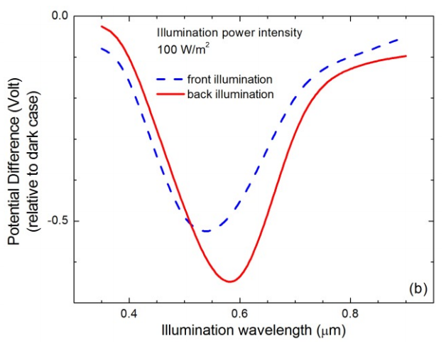
The improved sensitivity with BSI is also observed with the potential difference versus wavelength plots for both FSI and BSI cases as shown in Fig. 5 (b) with a comparison. It should be noted of that the results shown are based on the simple material structures as shown in Fig. 2. Complicated wavelength dependency might be expected when more materials especially like CFA are involved in the pixel buildup.
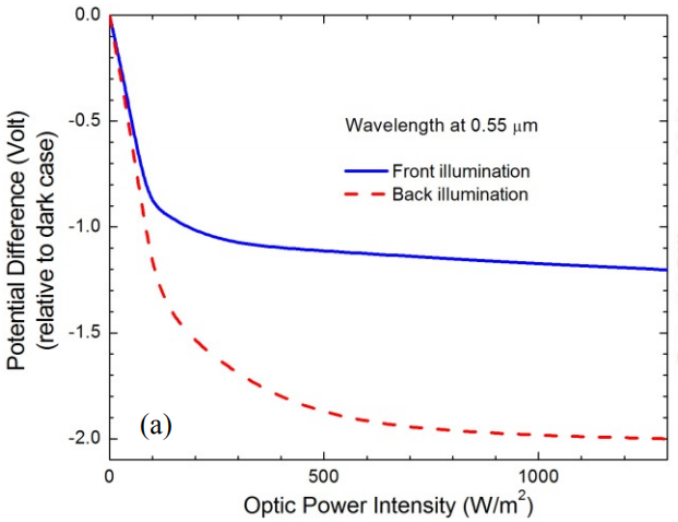
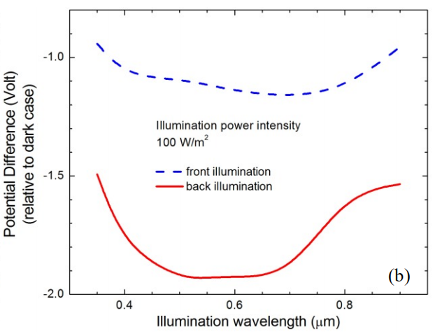
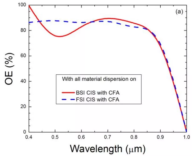
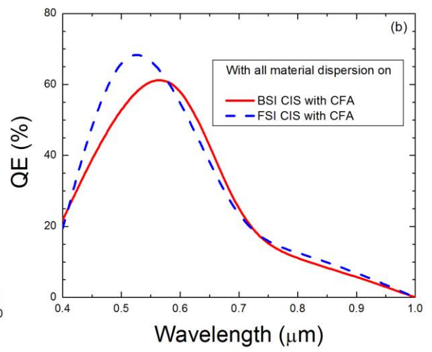
Whereas the aforementioned opto-electronic results support the BSI pixel design, it might be interesting to look from the solely the optical perspective with the results from FDTD. In Fig. 6 (a) and (b), respectively, the OE and QE results are compared between the BSI and FSI cases. Although the accuracy of FDTD simulation relies on large memory mesh with detailed and correct compilation of various material dispersion profiles, the results, especially the QE ones, indicate that the BSI pixel shows better sensitivity than FSI pixel at certain wavelength range for the pixel structures studied in this work, especially when full dispersion profiles (including SiO2) are considered for the front illumination case.
At this moment, we are also trying to get OE and QE comparison from optical TMM method. If the OE and QE obtained so shows the same traits of comparison between BSI and FSI as the FDTD OE and QE, it may prompt us to conclude that, for CIS, modeling solely based on optical OE and QE may not be enough to judge the actual pixel performance as in some situation, the case with low OE and QE may still have better sensitivity of transfer. The sensitivity is better represented by the potential difference with opto-electronic response as the OE or even the QE lacks the modeling mechanism for the charge-voltage conversion in the pixel [6]. This drives the need for the TCAD software with a full breadth of highly integrated process, optical and electronic modeling for CIS design and optimization.
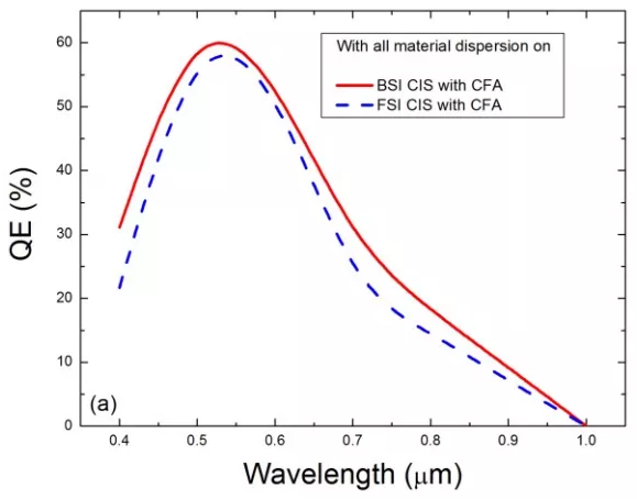
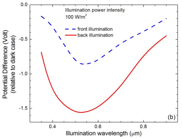
More work has been done to simulate the OE, QE and opto-electronic response by applying the CFA on the top and at the bottom of the structure as shown on Fig. 2 (a) and (b), respectively. The CFA is designed to have peak response near 0.55 µm with dispersion terms fitted from an assumed index data. The QE results are shown as in Fig. 7 (a) with the dispersion for all the materials included. From the QE results, the BSI pixel shows better performance than the FSI pixel, which is also supported by the potential difference versus wavelength plots for both FSI and BSI cases as shown in Fig. 7 (b), respectively, with a comparison.
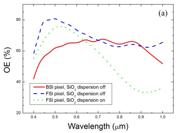
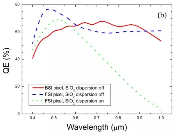
Next we present a 3D CIS structure built by CSuprem and the relevant comparison modeling of such a structure with FSI and BSI [7]. The schematic APS unit structure is similar to Fig. 1(b), but it is partially process-built with 9 mask layers (designed with Crosslight MaskEditor) as shown in Fig. 1 (c). The relevant process simulation is performed by Crosslight CSuprem. CSuprem simulation exports structure mesh, material together with doping subsequently to Crosslight APSYS. This simplified pixel unit does not include metal blocking aperture frame and the micro lens to reduce computation complexity. The CFA layer is on the top for FSI and at the bottom for BSI APS. The 3D device structures for both FSI and BSI are presented in Fig. 8 (a) and (b), respectively [7]. The relative optic power intensity of the typical 2D cut plane around photodiode and transfer gate is shown in Fig 9. (a) and (b) for FSI and BSI, respectively [7].
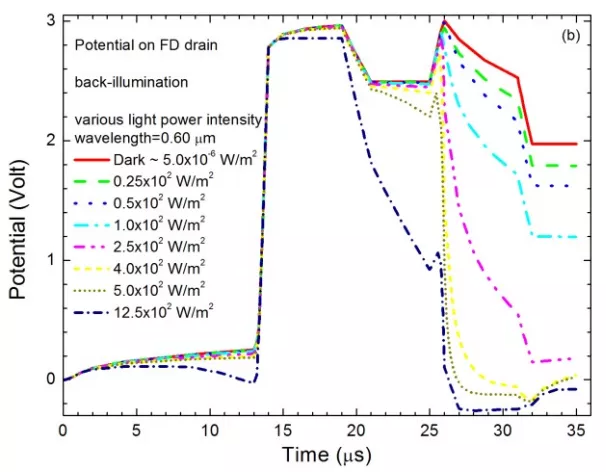
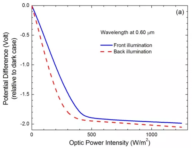
With the same operating illumination and bias time clock cycle as shown in Fig. 3, the potential difference (relative to dark case) on the FD after transfer stage (the end of the time evolution cycle) versus optical power intensity is shown in Fig. 10 (a) and (b) for FSI and BSI case respectively at 0.60 µm wavelength. The BSI case shows larger potential difference indicating improved sensitivity than the FSI case as shown in Fig. 11 (a). The improved sensitivity with BSI is also observed with the potential difference versus wavelength plots for both FSI and BSI cases within certain wavelength range as shown in Fig. 11 (b). The large enhancement is observed around 0.60 µm although we tried to design the CFA for 0.55 µm response. This means that the CFA needs to be re-designed for performance optimization. The peak response deviation might be also due to complexity of the other material involved in.
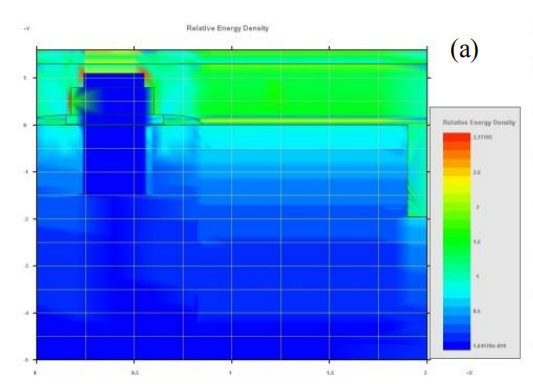
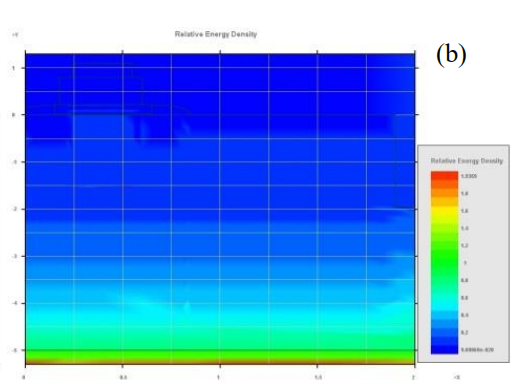

The OE and QE results for the pixels as shown in Fig. 8 has also been simulated with all material dispersion on. The results are shown in Fig. 12 (a) and (b), respectively. Although the OE and QE plots do not show quite the same feature, the results especially the QE one indicates that improved sensitivity can be achieved at certain wavelength range near the CFA response window for the BSI case. The simulated opto-electronic response is observed with deviation from designed CFA peak response which might be due to the inaccurate fitting of the various material dispersion terms as well as the numerical uncertainty. It is noted the results shown in this section for the CIS pixels built and processed by Csuprem is somehow deviated from the results presented in section 3. We attribute such partial discrepancy to the layout and the diffusion profiles, which are actually different for the CIS pixels shown in both sections. Nevertheless, the simulation for this section is under further examination. More optimization work is apparently needed on improved CFA design, the structure layout optimization together with the combined opto-electronic simulation. Further work relevant to CFA is cross-talk issues between (among) neighboring pixels. This would involve in more mesh and computation complexity.
The 3D modeling is reported for CMOS active pixel image sensors particularly by comparing FSI and BSI cases. The opto-electronic responses are presented versus various power intensity and illumination wavelength. The OE and QE results from FDTD modeling are also presented.
For appropriately designed sensor structure, it is shown that BSI case could achieve improved sensitivity within certain wavelength range comparing to the FSI pixel.
The modeling work also drives the need for the TCAD software with a full breadth of highly integrated process, optical and electronic modeling for CIS design and optimization. The presented results demonstrate a methodological and technical capability for 3D modeling optimization of complex CMOS image sensor.
Paper原文请查阅:
Yegao Xiao, Zhiqiang Li, Zhanming S. Li, “Modeling of InGaAs/AlGaAsSb APDs with high gain-bandwidth product,” Proc. SPIE 11498, Photonic Fiber and Crystal Devices: Advances in Materials and Innovations in Device Applications XIV, 114980R (20 August 2020); doi: 10.1117/12.2568197
Modeling of InGaAs/AlGaAsSb avalanche photodiodes (APDs) is presented in this work. Based on a drift-diffusion theory, the APD dark- and photo-current and multiplication gain are simulated. The frequency response and bandwidth are also computed based on a derived formalism by following the carrier transit analyses. Modeling results of I-V curves, multiplication gain, breakdown voltage, excess noise factor, -3dB bandwidth and gain-bandwidth product are demonstrated. Some results are compared with the experimental report. The APD performance is further evaluated with respect to two of the key design factors, the multiplication and the absorption layer thickness, respectively.
Keywords: Avalanche photodiodes, optoelectronics, device modeling and CAD software, optic fiber telecommunication
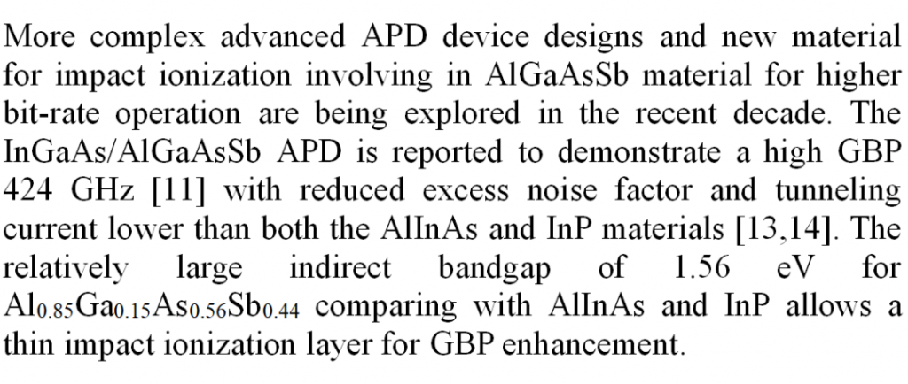
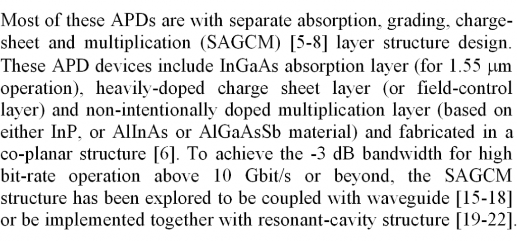
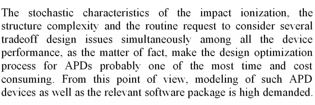
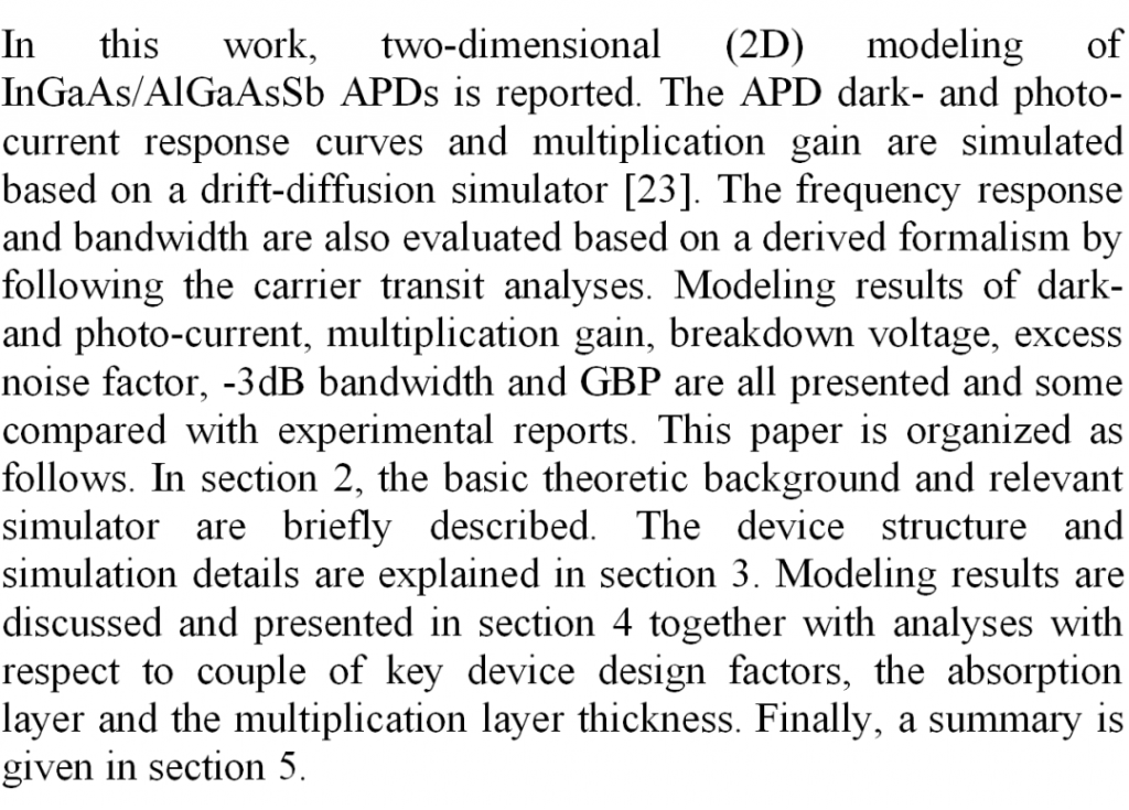








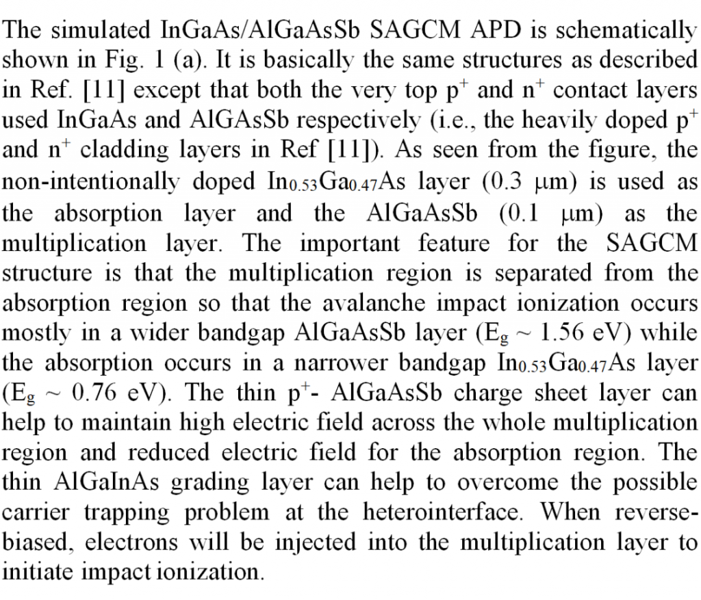
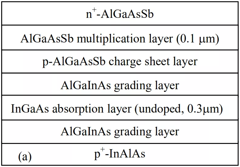
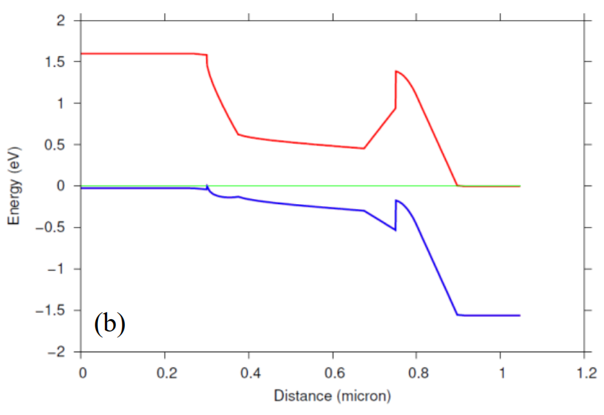
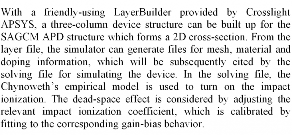

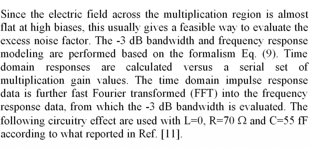
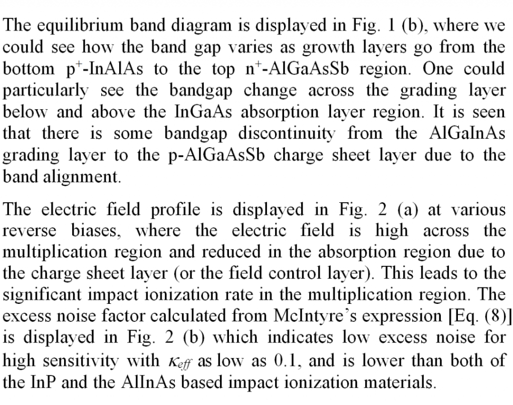
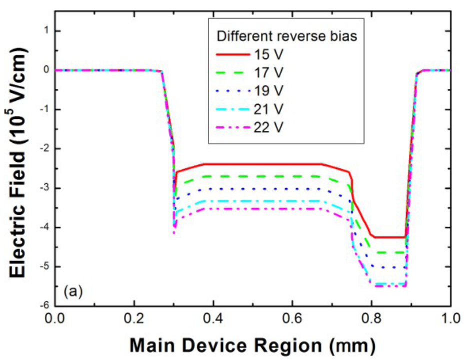
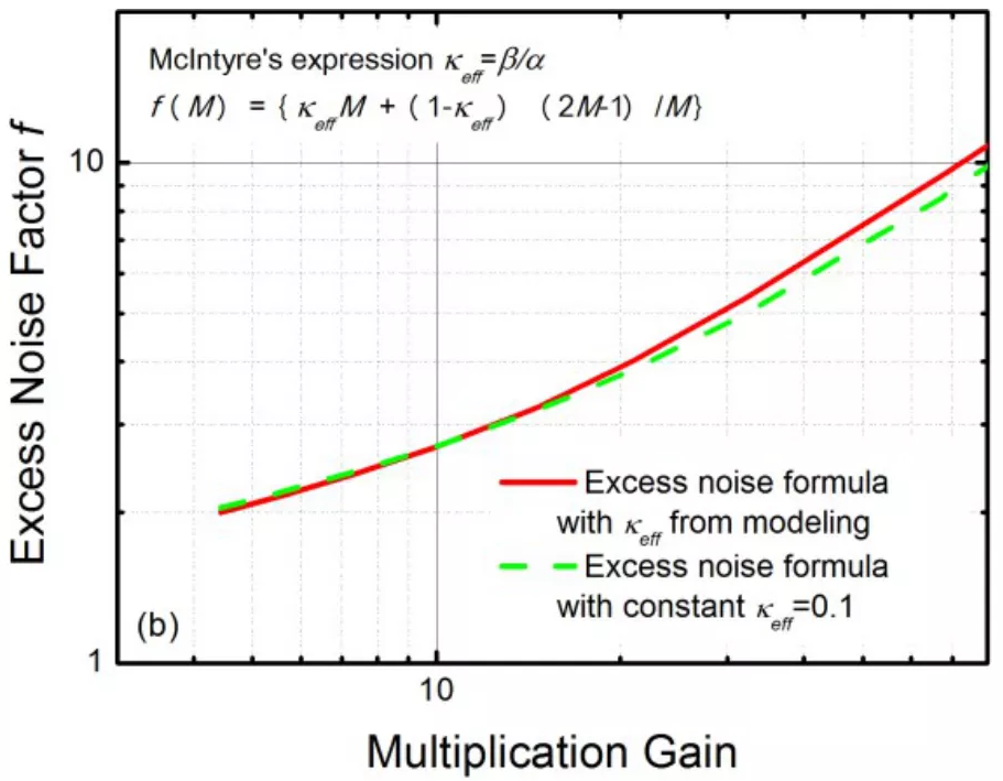
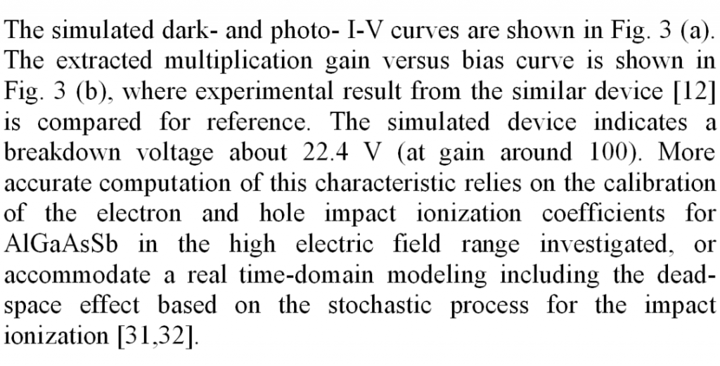
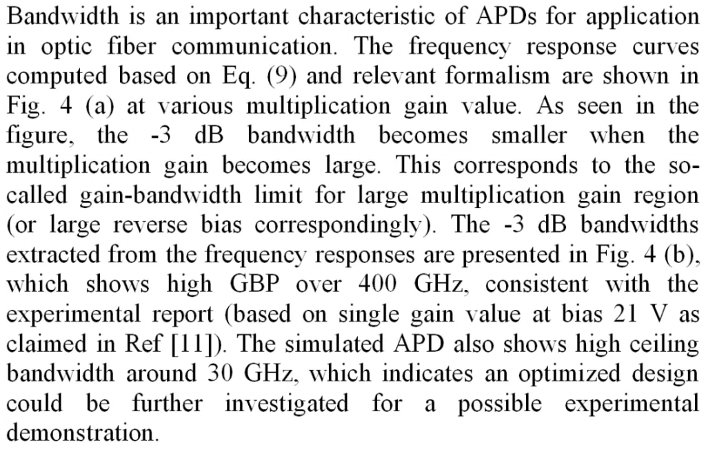
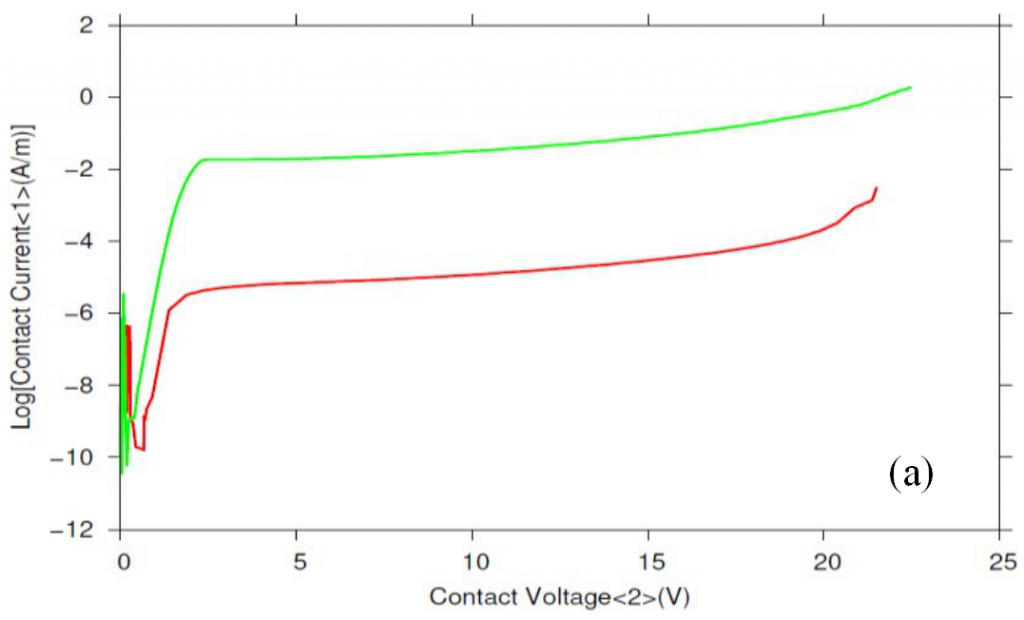
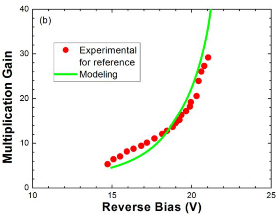
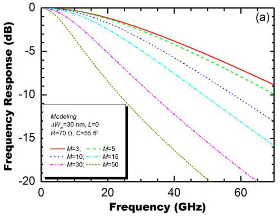
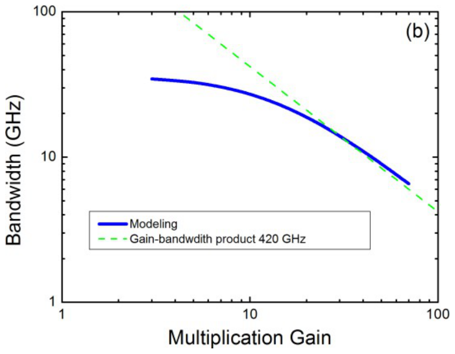

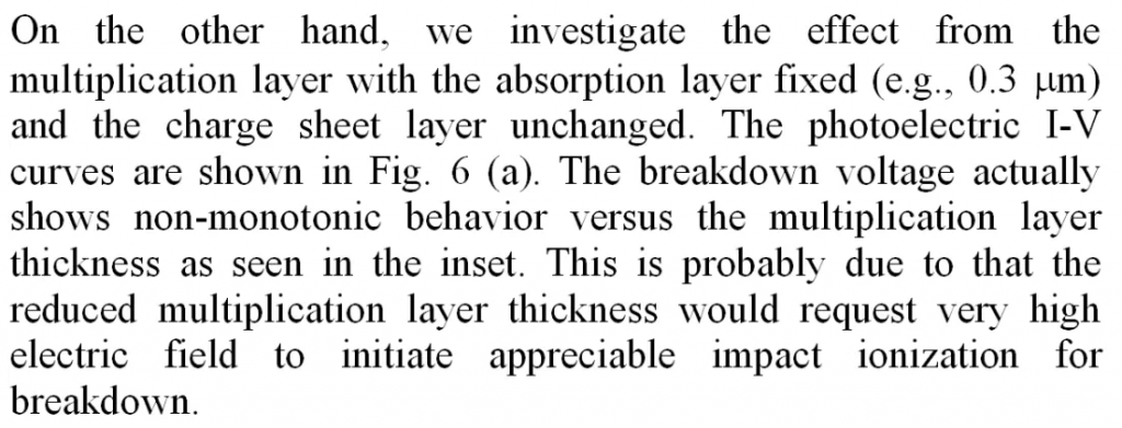
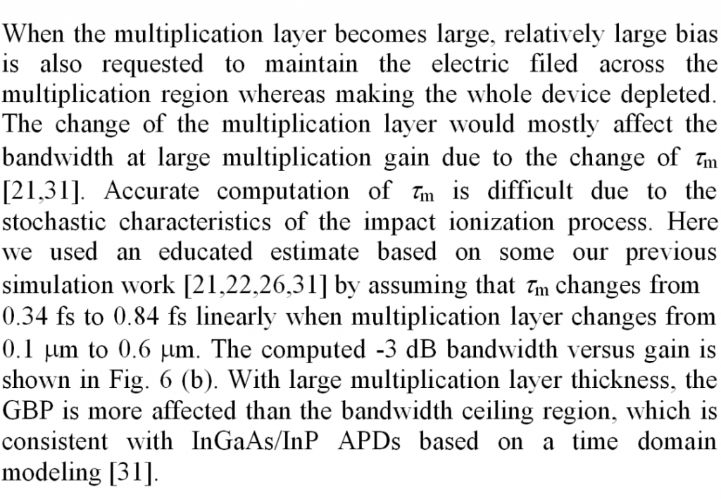
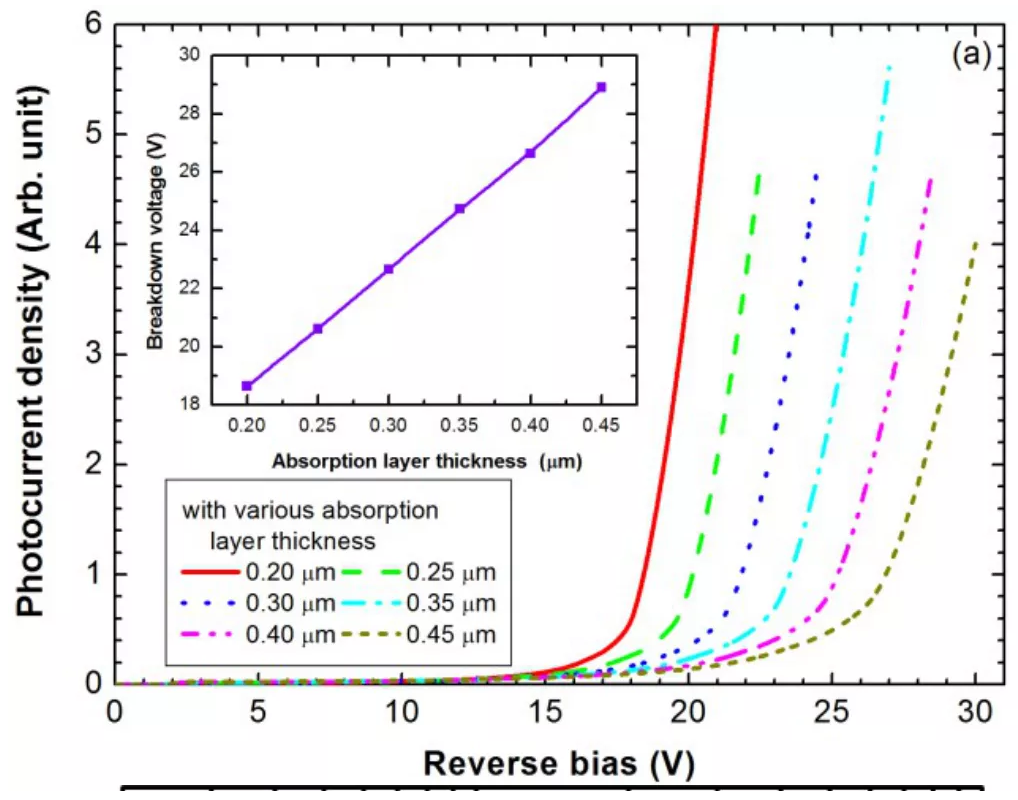
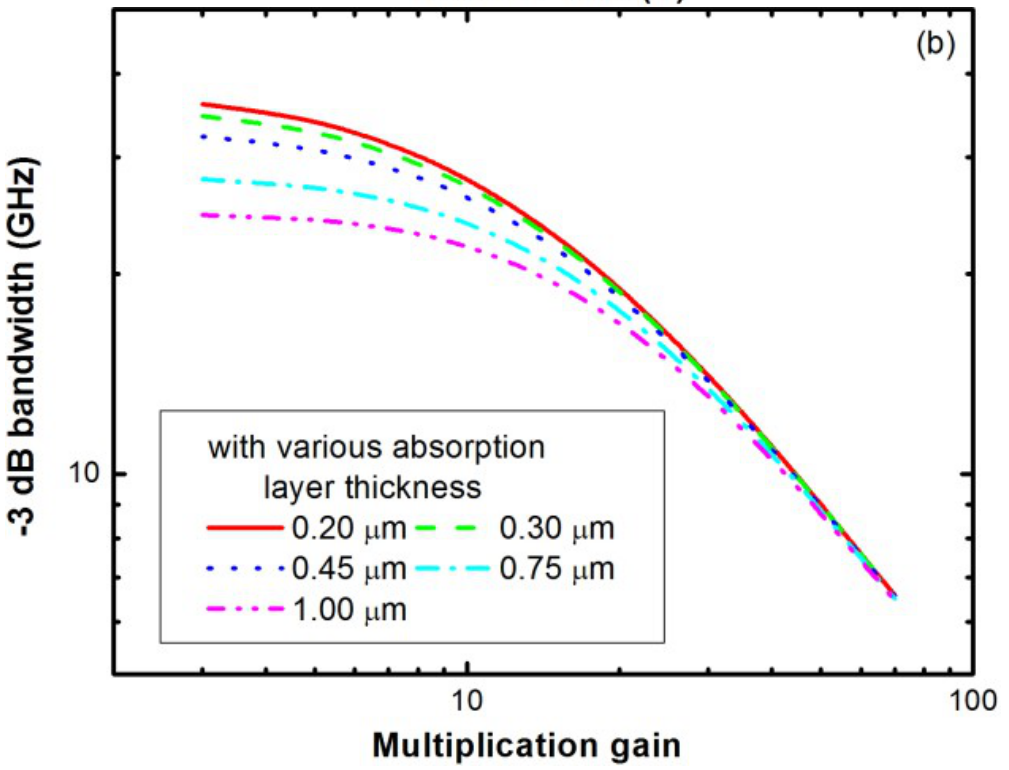
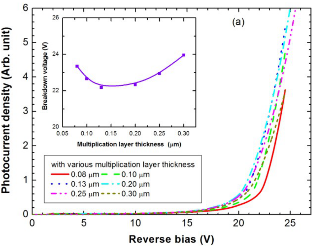
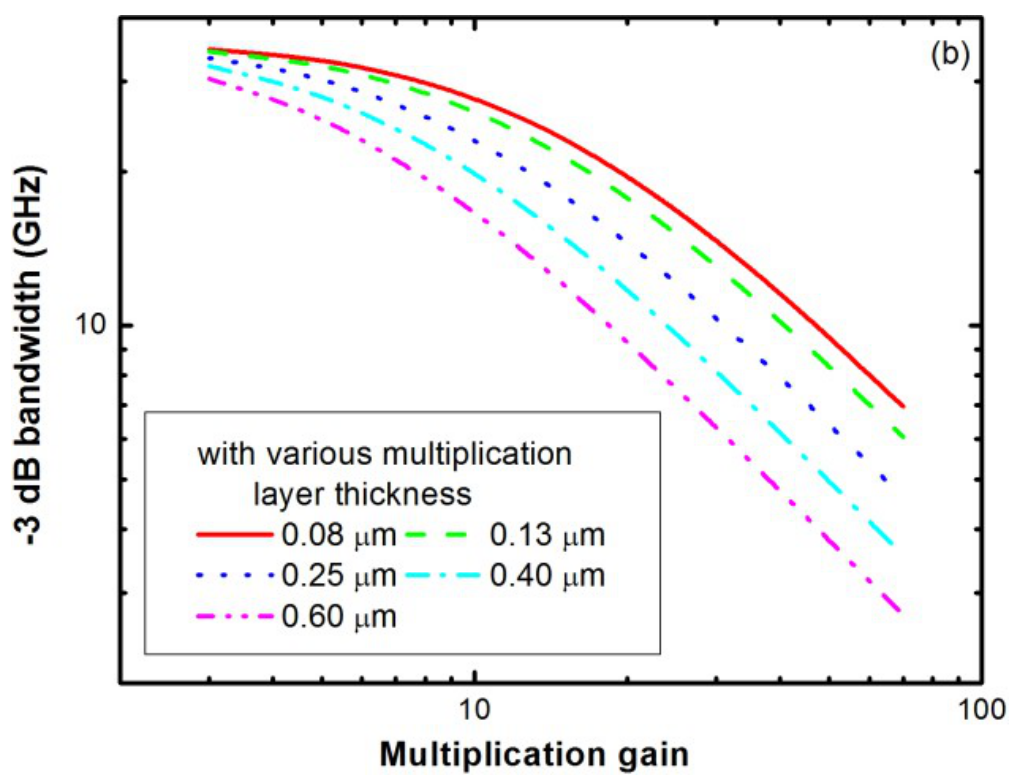

The 2D modeling of InGaAs/AlGaAsSb APDs is reported in this work. The APD dark- and photo-current and multiplication gain are simulated. The frequency response and bandwidth are also computed. Modeling results of I-V curves, multiplication gain, breakdown voltage, excess noise factor, -3dB bandwidth and gain-bandwidth product are demonstrated.
The device performance is further simulated with respect to two of the key factors, the multiplication layer and the absorption layer thickness, respectively. Some results are compared with the experimental report and some are further discussed based on the simulation work presented.
-记2020年11月5日,Crosslight相约交大李政道图书馆 – 一起感受科艺之美
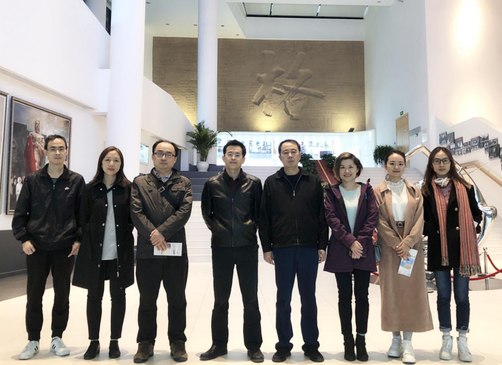
2020年11月5日 – 秋日午后和煦的阳光下,Crosslight上海分公司员工代表一行在创始人李湛明博士的带领下,前往坐落于上海交通大学闵行校区的李政道图书馆参观学习。
该场馆设计立足于李政道先生三十一岁便获得诺贝尔物理学奖的辉煌成就,取用“山”的意象,意在激励青年学生和科技工作者坚持不懈、勇攀科学高峰。
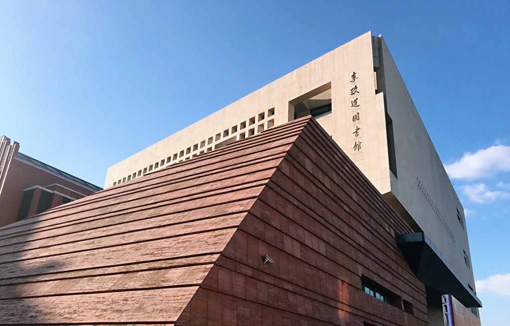
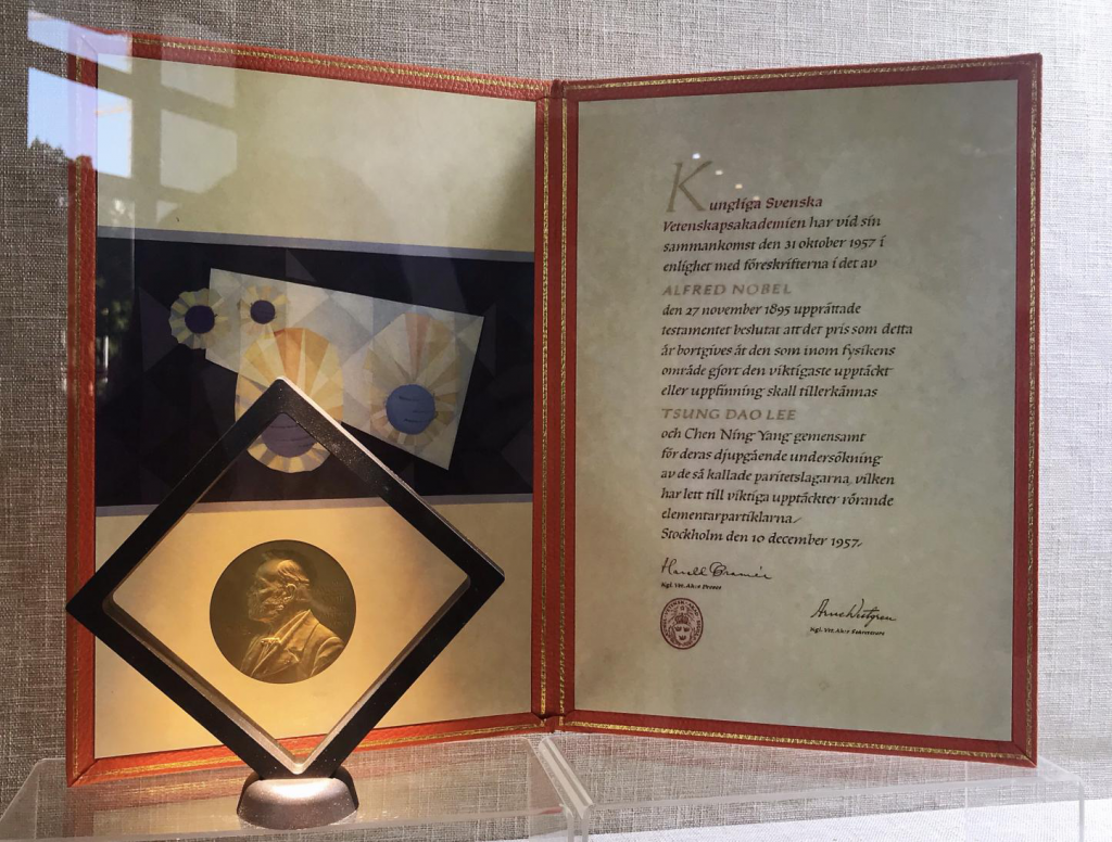
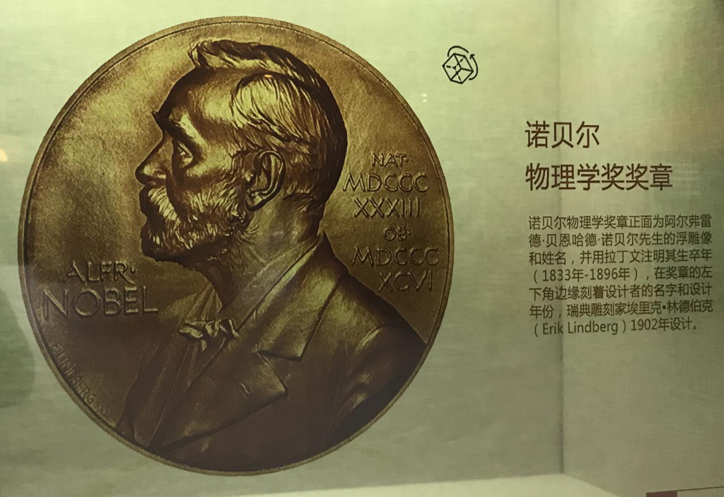
1957年,刚刚31岁的李政道与杨振宁因共同发现“弱相互作用中的宇称不守恒”获得“诺贝尔物理学奖”,两人成为历史上首获“诺贝尔物理学奖”的华人,而当时李政道是诺贝尔奖历史上第三年轻的获奖者。
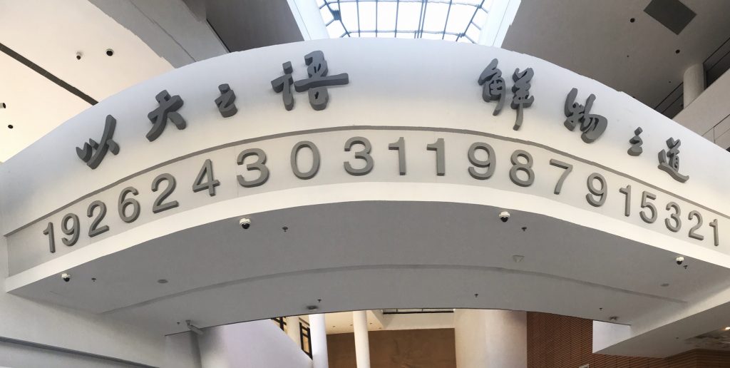
走进图书馆大厅,抬头便可以看见天桥上的一行遒劲有力的浮雕汉字———“以天之语,解物之道”,这八个由李政道先生亲笔书写的汉字是他一生的追求、感悟与心声,同时也是李馆陈列展览的主题。
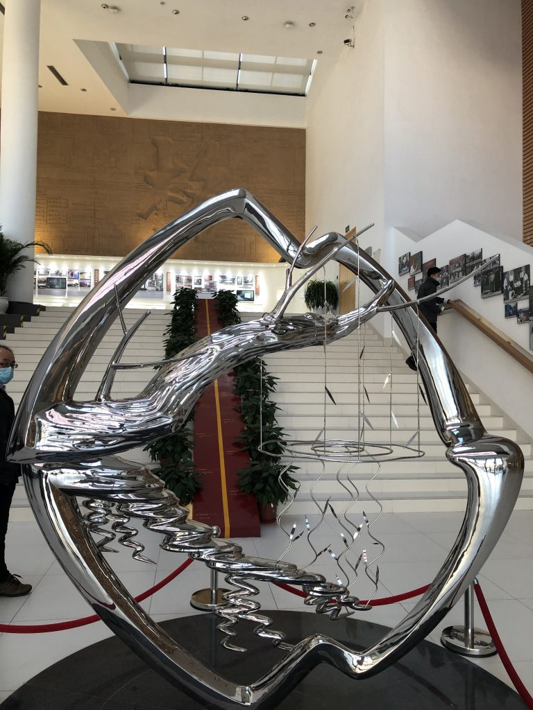
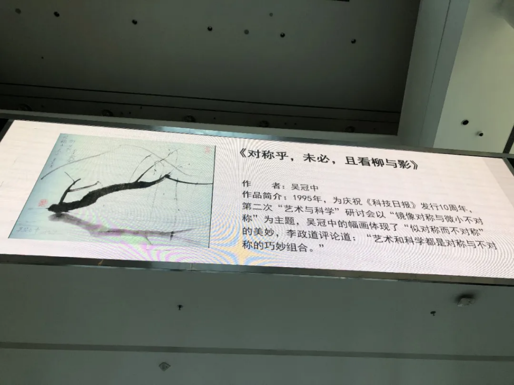
根据吴冠中先生的画作《对称呼,未必,且看柳与影、峰两侧》创作设计的雕塑,给参观者以视觉及情感上的震撼,全面展示李政道先生物理巨擘、赤子情怀、科艺双馨的人物特征。
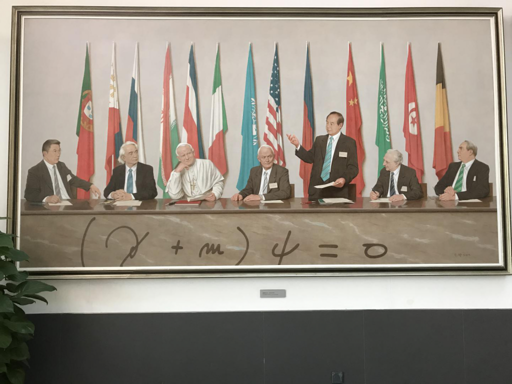
1993年5月8日,梵蒂冈教皇保罗二世(左三)为伽利略平反,并为其所受的不公正待遇向全球科学家道歉,李政道(右三)代表全球科学家接受教皇道歉。

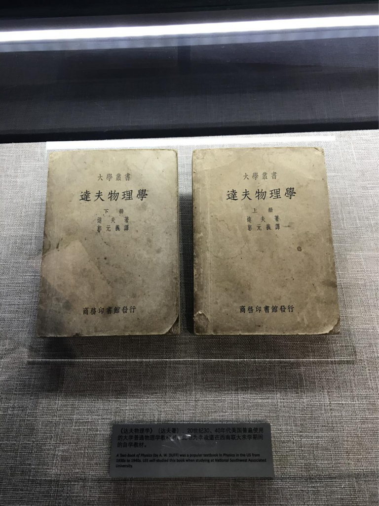
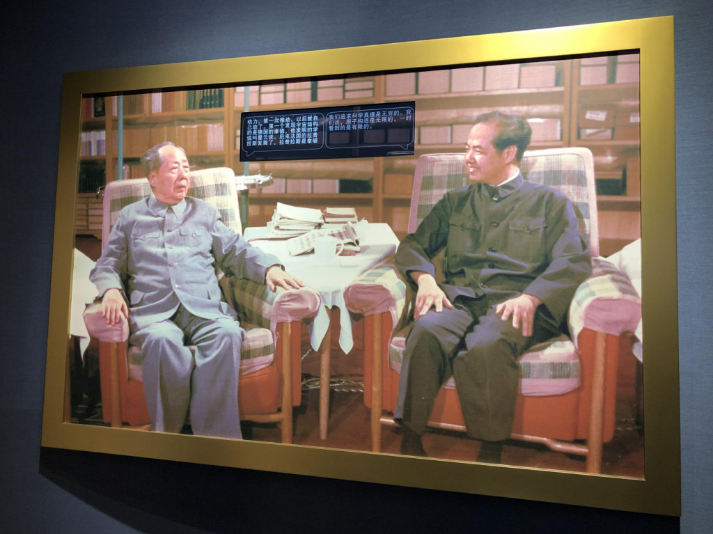
李政道在1974年第一次见到毛泽东,毛一见面就问他“为什么对称是重要的”,李政道抄起桌子上的本子和铅笔,给毛泽东作了一个小小的试验,他让铅笔在本子上来回滚动,然后对毛说,尽管没有一个瞬间是静止的,然而就整体而言,这个动力学的过程也有对称性;毛主席对什么是对称很有兴趣,他说,他一生经历的都是动荡,所以认为动是重要的。
李政道向毛主席建议要重视年轻科技人才的培养,进而促成‘少年班’的建立和全国性教学工作的恢复与发展。后又倡导成立了博士后流动站,选拔培养了大量物理方面的高级人才;
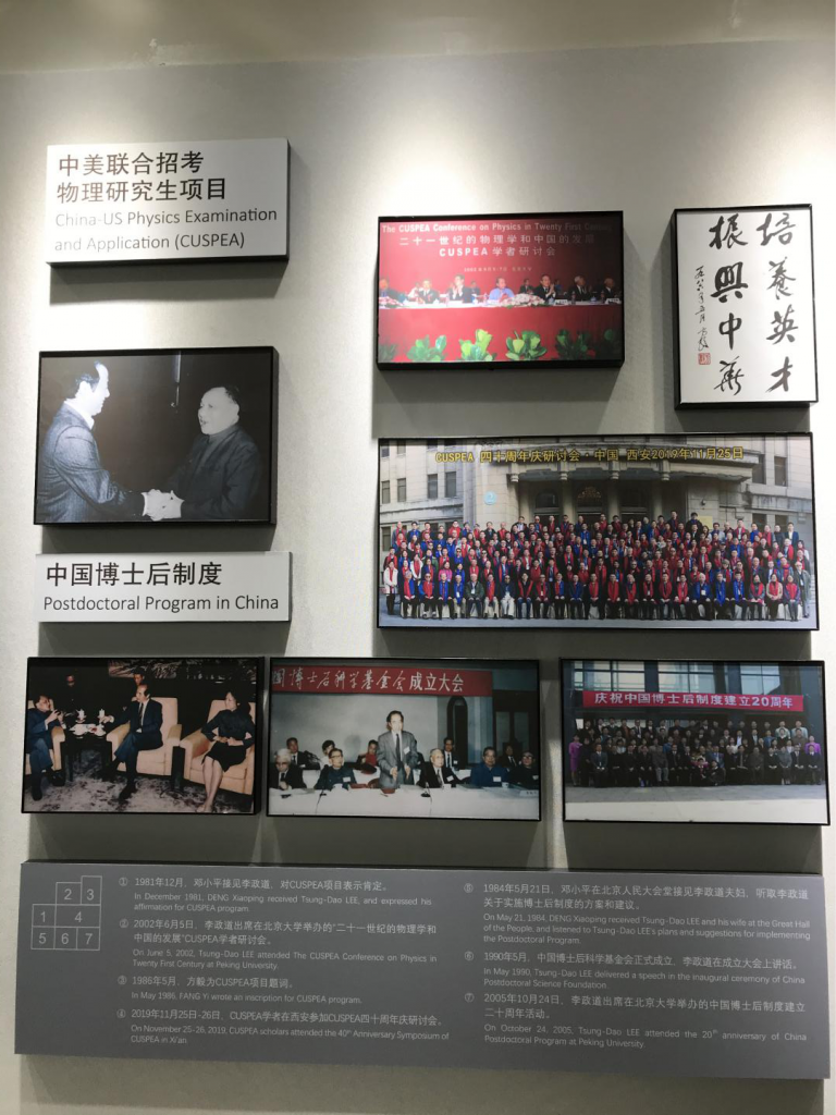
1980年,在中国没有托福和GRE、留学美国通道还未打开的情况下,李政道自己出资创建“中美联合招考物理研究生项目”,简称卡斯匹亚(CUSPEA)基金会。让中国学子得以留学美国。从1979-1989年差不多培养了1000个留学生。Crosslight公司创始人-李湛明博士就是CUSPEA基金会1981届前往留学的学生之一。
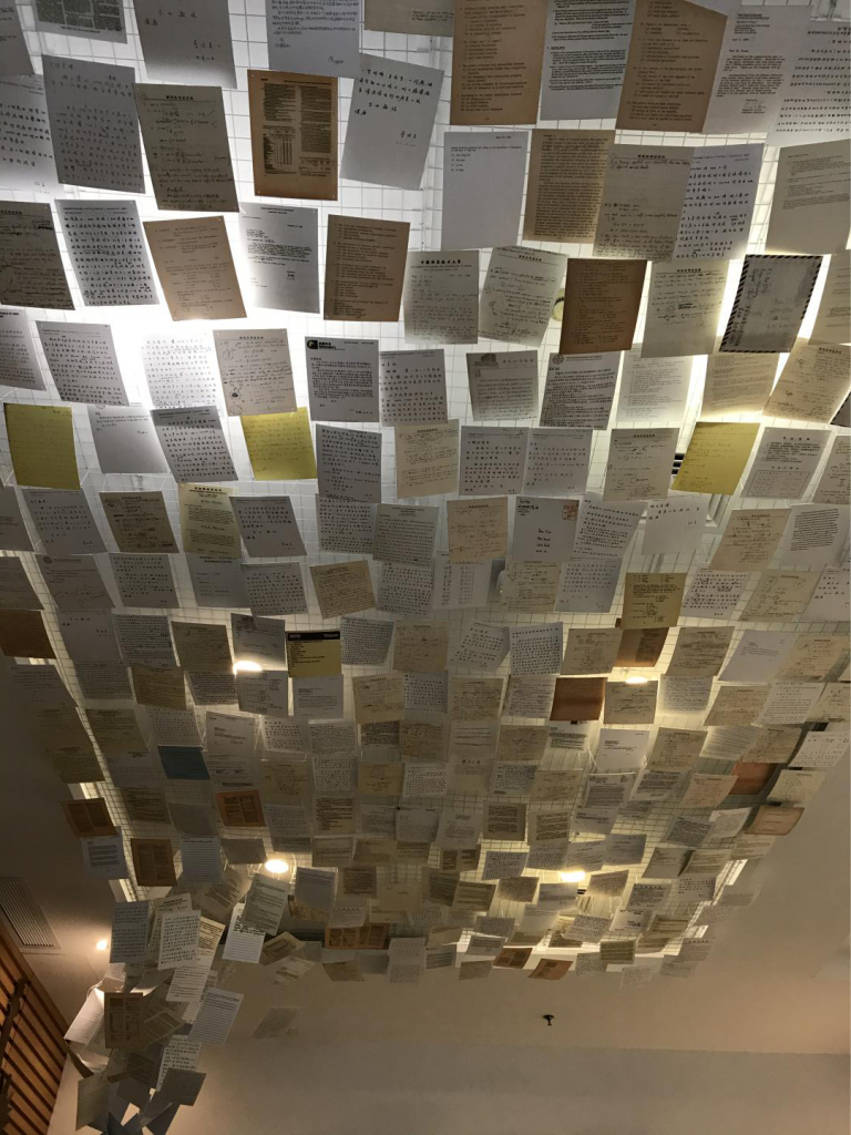
CUSPEA每年招收近百名中国学生,分布60余所一流大学,所有的招生往来信件都由李政道夫妇亲笔逐字书写,并推着小车辗转附近街区的各个邮筒投递;展馆的一角摆放的邮筒和信件展示了李政道先生对青年人才培养的重视和为之付出的艰辛努力;


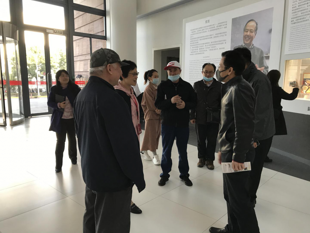
Crosslight员工代表跟随讲解员参观学习 :


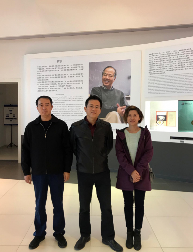
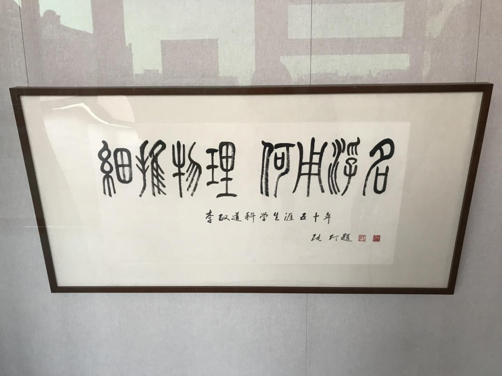
借用杜甫的诗句,同时也是李政道先生几十年科研之路的座右铭,作为今天参观学习的总结:
“细推物理须行乐,何用浮名绊此身。”
Crosslight公司也将秉承这样的务实理念,用心钻研技术、提高我们的产品和服务质量,和广大用户一起携手开创更美好的未来!