
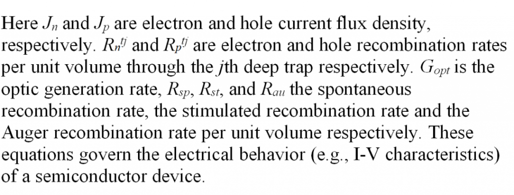
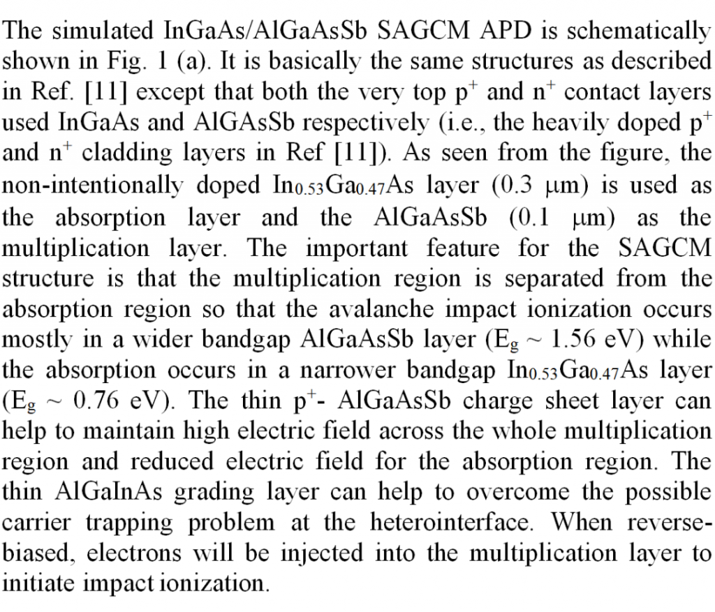
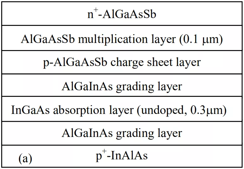
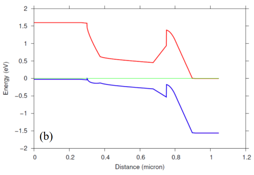
Yegao Xiao, Zhiqiang Li, Zhanming S. Li, “Modeling of InGaAs/AlGaAsSb APDs with high gain-bandwidth product,” Proc. SPIE 11498, Photonic Fiber and Crystal Devices: Advances in Materials and Innovations in Device Applications XIV, 114980R (20 August 2020); doi: 10.1117/12.2568197
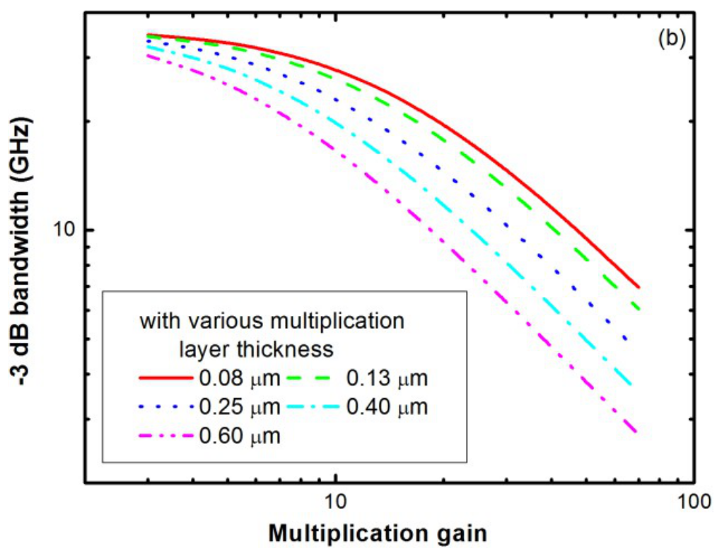
Modeling of InGaAs/AlGaAsSb avalanche photodiodes (APDs) is presented in this work. Based on a drift-diffusion theory, the APD dark- and photo-current and multiplication gain are simulated. The frequency response and bandwidth are also computed based on a derived formalism by following the carrier transit analyses. Modeling results of I-V curves, multiplication gain, breakdown voltage, excess noise factor, -3dB bandwidth and gain-bandwidth product are demonstrated. Some results are compared with the experimental report. The APD performance is further evaluated with respect to two of the key design factors, the multiplication and the absorption layer thickness, respectively.
Keywords: Avalanche photodiodes, optoelectronics, device modeling and CAD software, optic fiber telecommunication


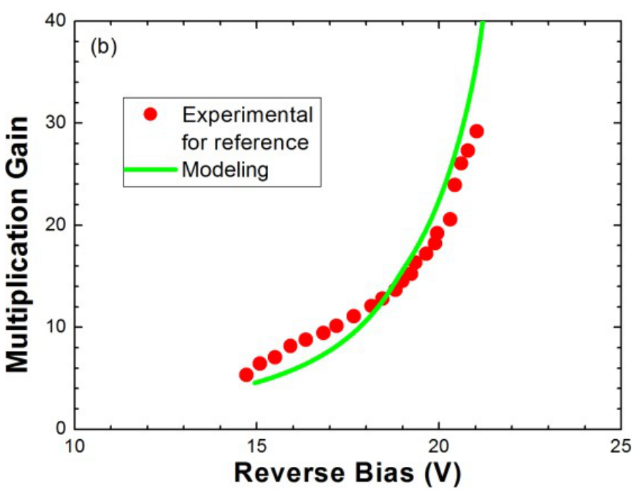
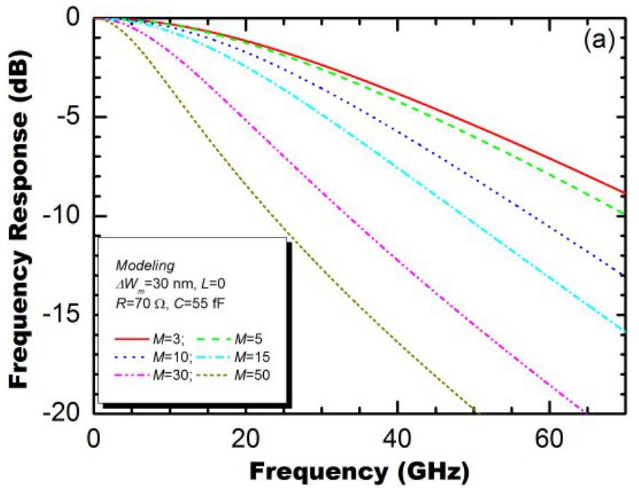
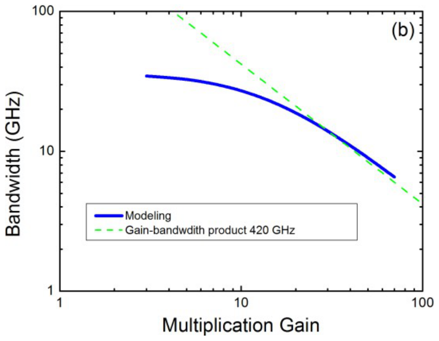


The 2D modeling of InGaAs/AlGaAsSb APDs is reported in this work. The APD dark- and photo-current and multiplication gain are simulated. The frequency response and bandwidth are also computed. Modeling results of I-V curves, multiplication gain, breakdown voltage, excess noise factor, -3dB bandwidth and gain-bandwidth product are demonstrated.
The device performance is further simulated with respect to two of the key factors, the multiplication layer and the absorption layer thickness, respectively. Some results are compared with the experimental report and some are further discussed based on the simulation work presented.