
Three-dimensional (3D) modeling is reported for CMOS active pixel image sensors particularly by comparing frontsurface and back-surface illumination. The opto-electronic responses are presented versus various power intensity and illumination wavelength.
The optical efficiency and quantum efficiency from FDTD modeling are also presented. For appropriately designed sensor structure, it is shown that back-surface illumination pixel could achieve improved sensitivity within certain wavelength range.
The presented results demonstrate a methodological and technical capability for 3D modeling optimization of complex CMOS image sensor.
Keywords:
CMOS image sensor, active pixel sensor, optoelectronics, device modeling and TCAD software, semiconductor devices
The complementary metal oxide semiconductor (CMOS) image sensors (CIS) are being widely used in various camera systems for automotive, consumer, industrial, & security imaging applications. The active pixel sensor (APS) has attracted increasing interest due to demand for miniaturized system-on-chip capability, low-power, and cost-effective imaging systems during the past two decades [1-3].
To increase the sensitivity without compromising the resolution for a front-surface illuminated (FSI) image sensor, various approaches including several photodiode structures such as the pinned photodiode (PPD) [3,4] have been proposed. Micro lens has also been fabricated to increase the light gathering power [5].
Other means like increasing the fill factor of the photo-electric conversion element as well as increasing the conversion gain of the source-follower amplifier etc have also been explored.
As a further technical development to overcome the benefit limitation of the aforementioned approaches, the back-surface illuminated (BSI) image sensor has attracted increasing attention due to enhanced sensitivity [6,7] and improved low-light performance.
It has been noted that a BSI sensor could theoretically cost less than a similar FSI one with the ability to collect more light.
For a similarly sized sensor to FSI one, the BSI array could offer higher resolution without the drop in low-light performance. Alternatively, for the same resolution and low-light capability, the BSI sensor could be achieved on a smaller chip with reduced costs. The BSI sensors have entered the commercialization market in recent years.
Due to the complexity of the 3D integration of photodiode and the optimization of metal layer distribution to maximize the sensitive area, 3D modeling together with effective optical modeling method such as finite difference time domain (FDTD) technique is indispensable [8,9]. An effective 3D modeling tool kit with full breadth covering process, optical and opto-electric response modeling is definitely requested.
In this work, based on Crosslight CSuprem and APSYS [10], we present 3D modeling of APS units designed for comparing the opto-electronic response between FSI and BSI pixels.
The paper is organized as flows. In section 2, brief software and methodological background for the modeling is described. In section 3, comparison is presented between two individual sensor pixels, one for FSI and the other for BSI, which are built by Crosslight LayerBuilder and simulated by APSYS.
Further in section 4, comparing results are presented between FSI and BSI for one individual sensor pixel, which is built and process simulated by Crosslight Csuprem together with Crosslight APSYS for the modeling the opto-electronic response. Summary and conclusion is finally given in section 5.
2.1 Software background
The Crosslight CSuprem [10] is a powerful 2D/3D process simulator, which is capable to interface with Crosslight APSYS. Its features include ion implantation, anisotropic and sacrificial etching, deposition, diffusion, annealing and oxidation etc. The Crosslight APSYS is general-purpose 2D/3D finite element analysis and modeling software for semiconductor devices [10].
The simulator solves several interwoven equations including the basic Poisson’s equation, and drift-diffusion current equations for electrons and holes. It includes many advanced physical models, friendly-using features and offers a flexible modeling and simulation environment. Advanced models include heterojunction models, (quantum) tunneling, hot carrier transport, trap dynamics, impact ionization and non-isothermal analysis etc. Important generation and recombination mechanisms, such as Shockley-Reed-Hall, spontaneous and Auger recombination, are taken into account. The software simulator provides several mobility model options from constant values to field dependent ones.
To simulate the optical effect of the complex CIS structure, Crosslight FDTD as well as interface techniques to other FDTD software is developed with APSYS. The graphic processing unit (GPU) solver is also implemented for fast computation capability.
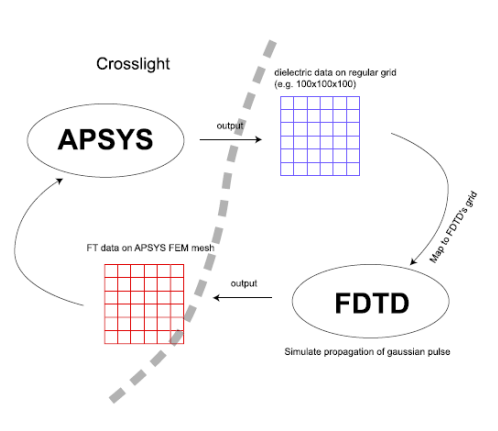
The schematic interface between FDTD and Crosslight APSYS is shown in Fig. 1 (a) [9].
The 3D grid uniform in each coordinate direction must be used for FDTD so there is a mapping of irregular device structure finite element data from/to Crosslight APSYS. In this work, all the optical efficiency (OE) and quantum efficiency (QE) results are from FDTD simulation of the relevant CIS structures. The OE is defined as the integration of the ratio of (ingoing flux-outgoing flux)/incident flux over device interface, where ingoing flux is the difference between the incident flux and the reflected flux upon the very beginning surface illuminated first. The QE is defined as integration of (absorption rate)*(relative energy intensity) across all the device 3D grid points. The OE does not care about which material absorbs light and has electron-hole pairs generated. The QE computation involves in more mesh memory than OE but provides more insight on the photo-electric conversion efficiency than the OE. The opto-electric response modeling like various contact terminal potential evolution versus operating time cycle is solely based on Crosslight APSYS with optical model involving in transfer matrix method (TMM) unless specified with alternative means.
2.2 Forming 3D CIS structures
The 3D CIS structures could be either formed by Crosslight LayerBuilder with multi-layers/columns by taking the advantage of the 3D-connect flow option. The 3D CIS formed by this way does not involve in process simulation. The 3D CIS structures could also be partially or fully process-built and simulated by Crosslight CSuprem with structure mesh, material together with doping exported and interfaced to Crosslight APSYS.
The latter is often used for complicated irregular geometrical design involving in multiple mask sets as designed by Crosslight Maskeditor. The schematic APS unit structure is similar to Ref. [1-3,5,7,9] including a pinned photodiode, a transfer (TX) gate, and a reset (RST) gate.
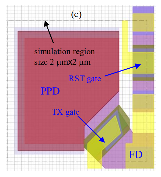
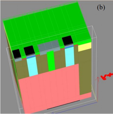
Due to the thinning request and also for reducing the mesh size, we assume 5-um-thick p-type starting substrate. The typical CIS schematic (regular geometry) with Crosslight LayerBuilder only is shown in Fig. 1 (b) whereas the detailed unit component deployment (as generated by Crosslight MaskEditor with 9 mask layers and subsequent CSuprem process simulation) is schematically shown in Fig. 1 (c).
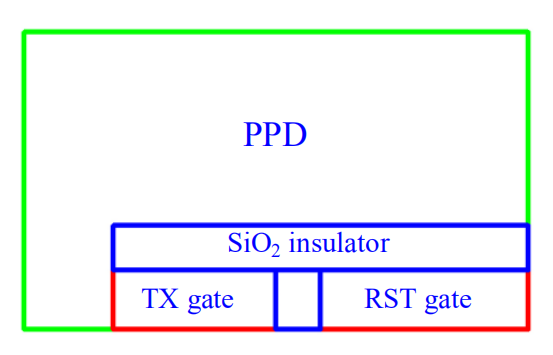
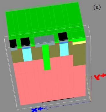
In this section, we compare two sensor structures, one for FSI and the other for BSI. These two pixels are built by APSYS LayerBuilder only according to the schematics shown in Fig. 1 (b). These two structures with 3D connect-flow are shown in Fig. 2 (a) and (b) for FSI and BSI, respectively. Trench insulators are inserted among PPD, TX gate and RST gate. Most of the front surface is simply assumed to be covered with thin SiO2 as anti-reflection coating layer whereas the back surface is the (thinned) wafer base. For simplicity, no color filter array (CFA) is included for these two structures for most of the modeling work except for comparison presented at the end of this section.
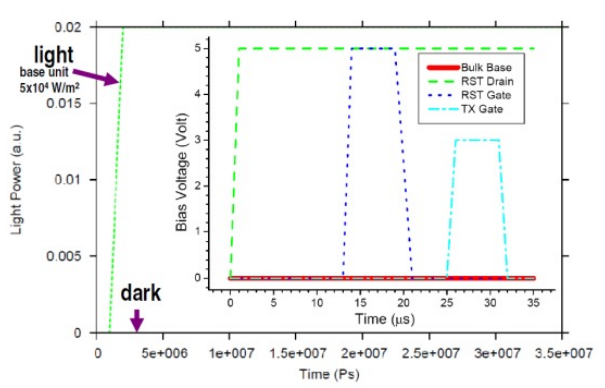
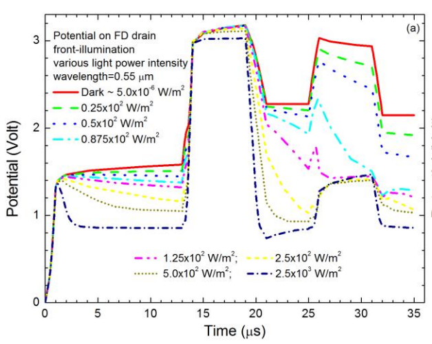
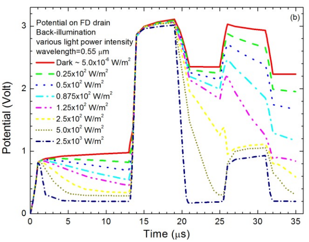
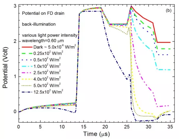
With the operating illumination and bias time clock cycle (reset at first and then transfer) as shown in Fig. 3, the evolution of the potential on the floating drain (FD) versus time is shown in Fig. 4 (a) and (b) respectively for FSI and BSI pixel, respectively. With increasing power intensity, the potential on FD shows increasingly large difference relative to the dark case at the transfer stage. When the power intensity reaches certain level, the overshot-effect becomes dominant at the transfer stage. Although not presented here, the results during the modeling process also indicate the 3D current crowding effect, like poor sensitivity.
This is accompanied by small or unchanged potential difference relative to the dark case at the transfer stage with appropriate optical power intensity of illumination when too-wide PPD range is set along the transfer gate and with poor trench insulation.
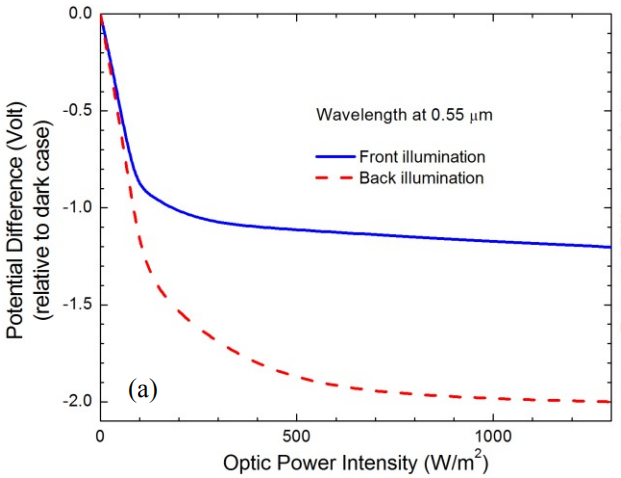
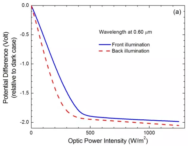
The potential difference (relative to dark case) on the FD after transfer stage (the end of the time evolution cycle) versus optical power intensity is shown in Fig. 5 (a) for BSI and FSI pixels by comparison at 0.55 µm wavelength. The BSI pixel shows larger potential difference indicating improved sensitivity than the FSI pixel.
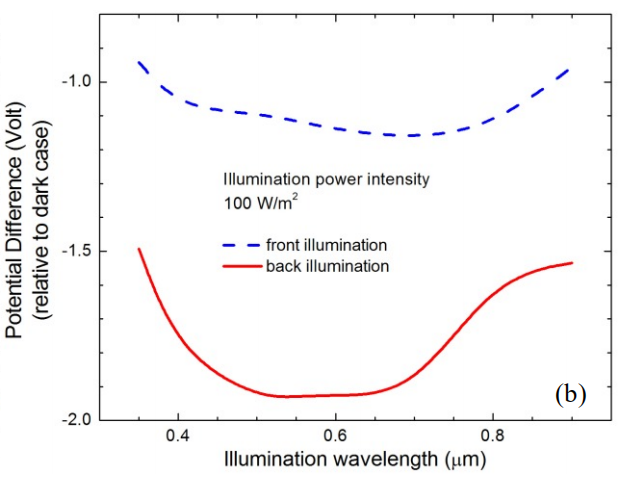
The improved sensitivity with BSI is also observed with the potential difference versus wavelength plots for both FSI and BSI cases as shown in Fig. 5 (b) with a comparison. It should be noted of that the results shown are based on the simple material structures as shown in Fig. 2. Complicated wavelength dependency might be expected when more materials especially like CFA are involved in the pixel buildup.
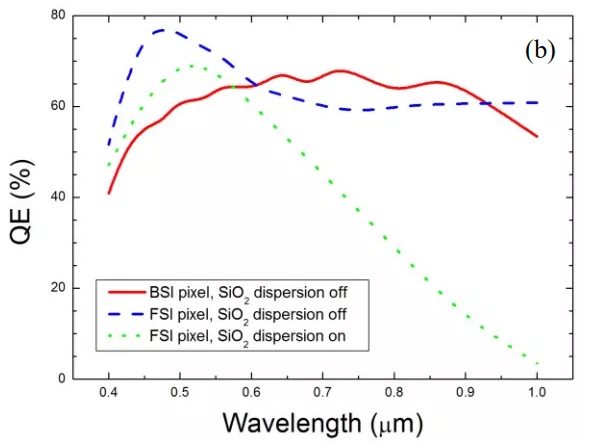
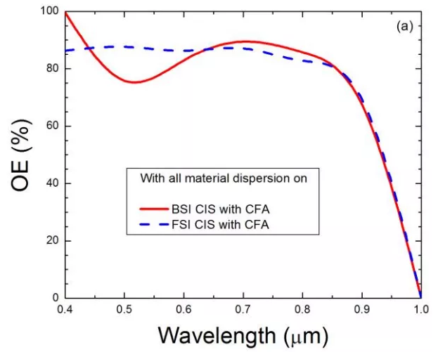
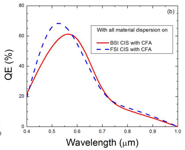
Whereas the aforementioned opto-electronic results support the BSI pixel design, it might be interesting to look from the solely the optical perspective with the results from FDTD. In Fig. 6 (a) and (b), respectively, the OE and QE results are compared between the BSI and FSI cases. Although the accuracy of FDTD simulation relies on large memory mesh with detailed and correct compilation of various material dispersion profiles, the results, especially the QE ones, indicate that the BSI pixel shows better sensitivity than FSI pixel at certain wavelength range for the pixel structures studied in this work, especially when full dispersion profiles (including SiO2) are considered for the front illumination case.
At this moment, we are also trying to get OE and QE comparison from optical TMM method. If the OE and QE obtained so shows the same traits of comparison between BSI and FSI as the FDTD OE and QE, it may prompt us to conclude that, for CIS, modeling solely based on optical OE and QE may not be enough to judge the actual pixel performance as in some situation, the case with low OE and QE may still have better sensitivity of transfer. The sensitivity is better represented by the potential difference with opto-electronic response as the OE or even the QE lacks the modeling mechanism for the charge-voltage conversion in the pixel [6]. This drives the need for the TCAD software with a full breadth of highly integrated process, optical and electronic modeling for CIS design and optimization.
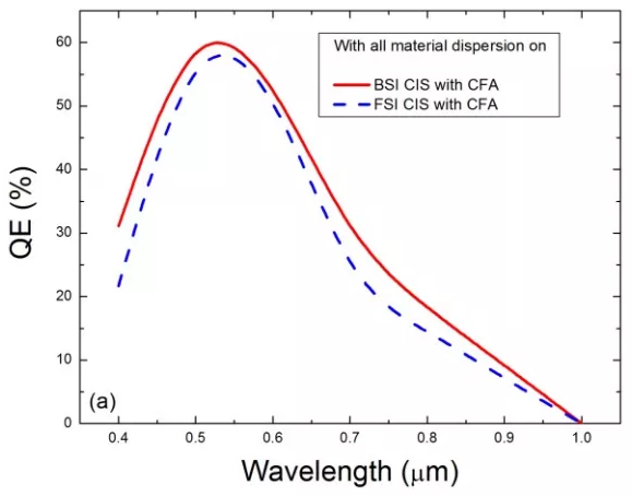
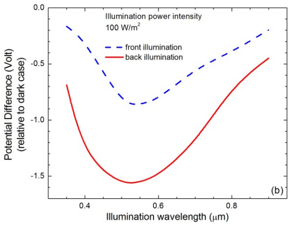
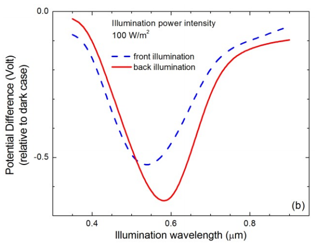
More work has been done to simulate the OE, QE and opto-electronic response by applying the CFA on the top and at the bottom of the structure as shown on Fig. 2 (a) and (b), respectively. The CFA is designed to have peak response near 0.55 µm with dispersion terms fitted from an assumed index data. The QE results are shown as in Fig. 7 (a) with the dispersion for all the materials included. From the QE results, the BSI pixel shows better performance than the FSI pixel, which is also supported by the potential difference versus wavelength plots for both FSI and BSI cases as shown in Fig. 7 (b), respectively, with a comparison.
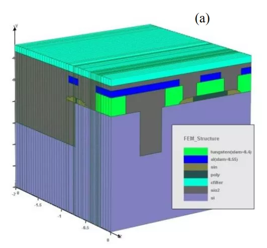
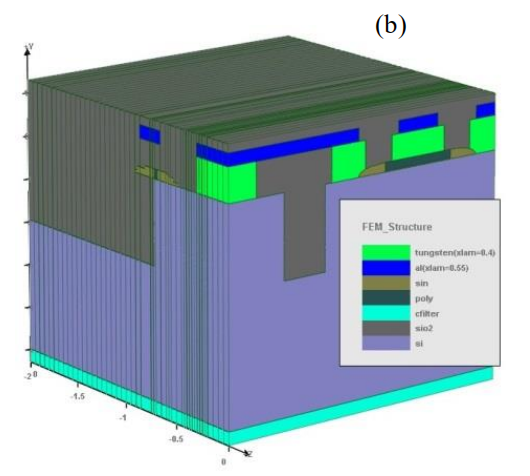
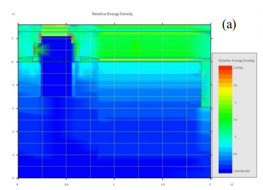
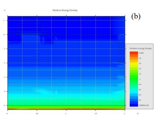
Next we present a 3D CIS structure built by CSuprem and the relevant comparison modeling of such a structure with FSI and BSI [7]. The schematic APS unit structure is similar to Fig. 1(b), but it is partially process-built with 9 mask layers (designed with Crosslight MaskEditor) as shown in Fig. 1 (c). The relevant process simulation is performed by Crosslight CSuprem. CSuprem simulation exports structure mesh, material together with doping subsequently to Crosslight APSYS. This simplified pixel unit does not include metal blocking aperture frame and the micro lens to reduce computation complexity. The CFA layer is on the top for FSI and at the bottom for BSI APS. The 3D device structures for both FSI and BSI are presented in Fig. 8 (a) and (b), respectively [7]. The relative optic power intensity of the typical 2D cut plane around photodiode and transfer gate is shown in Fig 9. (a) and (b) for FSI and BSI, respectively [7].
With the same operating illumination and bias time clock cycle as shown in Fig. 3, the potential difference (relative to dark case) on the FD after transfer stage (the end of the time evolution cycle) versus optical power intensity is shown in Fig. 10 (a) and (b) for FSI and BSI case respectively at 0.60 µm wavelength. The BSI case shows larger potential difference indicating improved sensitivity than the FSI case as shown in Fig. 11 (a). The improved sensitivity with BSI is also observed with the potential difference versus wavelength plots for both FSI and BSI cases within certain wavelength range as shown in Fig. 11 (b). The large enhancement is observed around 0.60 µm although we tried to design the CFA for 0.55 µm response. This means that the CFA needs to be re-designed for performance optimization. The peak response deviation might be also due to complexity of the other material involved in.

The OE and QE results for the pixels as shown in Fig. 8 has also been simulated with all material dispersion on. The results are shown in Fig. 12 (a) and (b), respectively. Although the OE and QE plots do not show quite the same feature, the results especially the QE one indicates that improved sensitivity can be achieved at certain wavelength range near the CFA response window for the BSI case. The simulated opto-electronic response is observed with deviation from designed CFA peak response which might be due to the inaccurate fitting of the various material dispersion terms as well as the numerical uncertainty. It is noted the results shown in this section for the CIS pixels built and processed by Csuprem is somehow deviated from the results presented in section 3. We attribute such partial discrepancy to the layout and the diffusion profiles, which are actually different for the CIS pixels shown in both sections. Nevertheless, the simulation for this section is under further examination. More optimization work is apparently needed on improved CFA design, the structure layout optimization together with the combined opto-electronic simulation. Further work relevant to CFA is cross-talk issues between (among) neighboring pixels. This would involve in more mesh and computation complexity.
The 3D modeling is reported for CMOS active pixel image sensors particularly by comparing FSI and BSI cases. The opto-electronic responses are presented versus various power intensity and illumination wavelength. The OE and QE results from FDTD modeling are also presented.
For appropriately designed sensor structure, it is shown that BSI case could achieve improved sensitivity within certain wavelength range comparing to the FSI pixel.
The modeling work also drives the need for the TCAD software with a full breadth of highly integrated process, optical and electronic modeling for CIS design and optimization. The presented results demonstrate a methodological and technical capability for 3D modeling optimization of complex CMOS image sensor.
Paper原文请查阅: